
Table of Contents
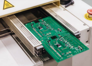
PCB etching is one of the crucial processes in PCB design that allows for maximum accuracy and reliability in today’s electronics. The process involves removing certain layers of copper from a board to form intricate pathways connecting electronic components. It is a process by which manufacturers can begin to gain some insight into how the process operates and what techniques are involved in ensuring such high-quality circuits, whether they be consumer gadgets or industrial machinery.
Meaning of Etching of PCB in Electronics Manufacturing
PCB etching in manufacturing is quite essential when circuits have to be fabricated. It gives a smooth process of running circuits without any signal interference and electrical short-circuiting. The risks will be the risks to malfunctions of a device because the risks are minimized while there is adequate control on etching for circuit paths to remain intact in encouraging a more convenient interconnection and reliability. This level of attention to detail is crucial in that process, particularly for the industries of telecommunications, automotive, and healthcare, where small faults mean much.
Select Techniques for PCB Etching
It can be performed through various methods depending on the complexity and precision required. Some of the most common techniques include:
Wet Etching: This is a chemical etch solution, usually acidic. It dissolves copper outside the protective mask coating a PCB. Therefore, wet etching can only remove exposed regions of copper. It is common in large-scale PCB productions but requires safe handling of chemicals and disposal methods.
Dry Etching: Through the use of gases and plasma instead of chemicals, this process erodes the exposed copper. Dry etching is unlike wet etching but is better controlled and much more precise for smaller PCBs that are used usually in advanced electronics and microelectronics.
Laser Etching: In the last decades, laser technology has come up to achieve even a greater degree of precision while etching PCBs. Laser etching is a non-contact process and so precise that the chance of contamination is minimal and much material waste is avoided as well. This method proves suitable for complex circuits requiring very fine patterns that normal methods cannot achieve.
Safety and Environmental Considerations in PCB Etching
Etching of PCB, especially with chemicals, requires excellent safety precautions. The proper use of protective gear and the proper disposal should be able to minimize the adverse impact on the environment from hazardous wastes. With a better understanding of environmental requirements, manufacturing companies more and more for greener alternatives or methods to recycle the leftovers of etching processes.
Future of Etching of PCB
Improving the technology in etching PCB provides a means for more effective and environmentally friendly processes. Laser etching is now in high demand due to precision and minimal waste generation. Innovations in chemical-free etching solutions may further reduce the environmental impact of etching of PCB, thereby making the process more sustainable.
Final Remarks
PCB etching is an indispensable process in the production of reliable and high-performing circuits. From wet and dry etching to the highly advanced laser technology, every method has its specific benefits best suited for a certain application. Further developments in techniques for etching of PCB will enable manufacturers to construct more complex circuits based on present demands for high precision and quality. Continued refinement in the practice of etching of PCB can help the electronics industry to innovate and, therefore, advance the high-tech technology.
0