
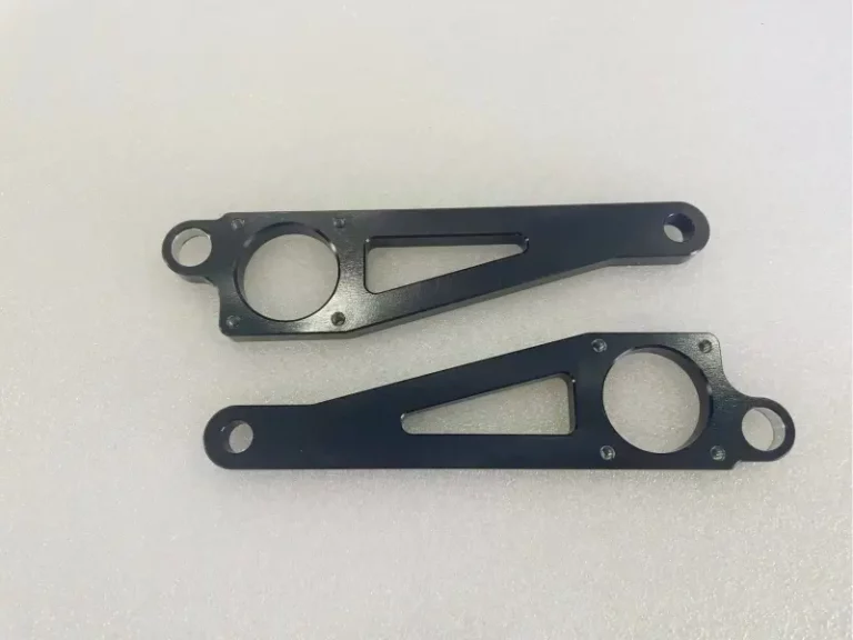
Aluminum alloys have become indispensable in modern industrial applications due to their lightweight...
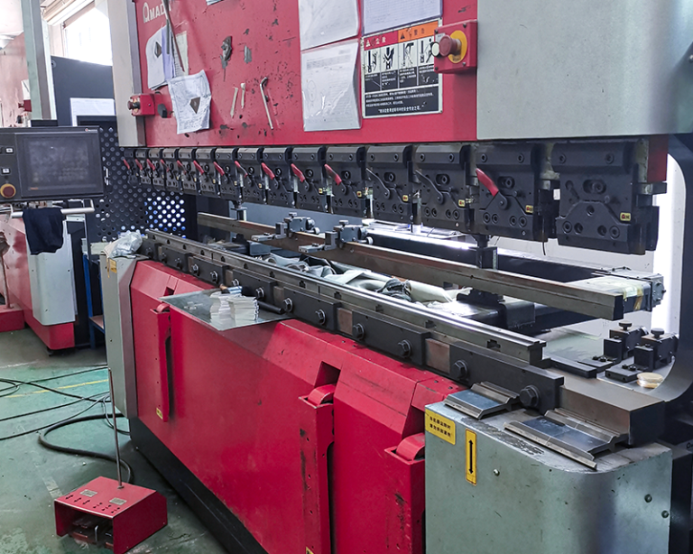
As an important link in the manufacturing industry, sheet metal processing is widely used in multiple...
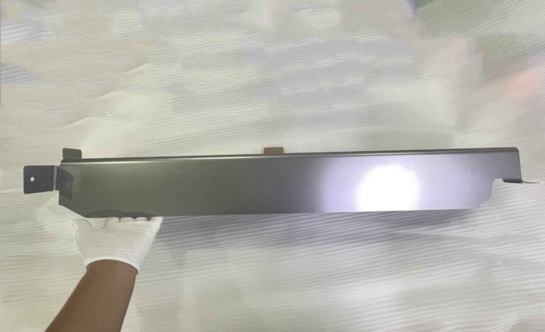
Precision-Engineered Custom Components
For many industries, the need for custom parts is a common requirement....
Table of Contents
Introduction
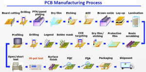
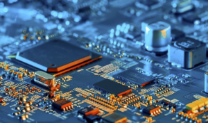
This blog will help you learn the PCB Fab Process. You will see tips on drilling, plating, and finishing. These steps are key. The goal is to make strong and reliable boards. Follow the guide closely.
What Are the Fundamental Steps in PCB Fabrication?
- Design
Start with the layout. The software makes a map. Traces are lines. Pads are locations for components. Layers stack up. The Gerber files contain the plan. Use CAM software. Layers are connected through connectors and vias. DRC checks for errors. Ensure that all pathways are clear. Each step counts. Design rules keep things running. Double-check everything. Transmit files to the fab shop. - Material Selection
Choose the right materials. Copper is for traces. FR4 is the base. Solder mask covers copper. Silkscreen labels parts. Each part has a function. Thickness matters. Check the datasheet.
Glass transition temp is important. The materials used should also correspond with the design used in the project. Pick parts that fit. Ensure good quality. The right choice contributes to the process. Test each material. - Patterning
Start with copper-clad boards. Photoresist coats the surface. UV light should be used to expose the pattern. A developer solution is used by the developer to wash out the soft photoresist.
Hardened areas stay. Copper can be seen through the pattern. Create paths for current. Pattern is key. Every trace has a role to play. The photo plotter creates the image. Clean edges are important. Patterns guide the process. - Etching
Place the board in the etching tank. Ferric chloride dissolves exposed copper. Only covered areas stay. Wipe off the board after the etching is complete. Check for missing paths. Etching makes the circuit. Each trace must connect. Timing is crucial. Remove extra copper. Etching is precise. Paths form connections. Inspect the etched board. - Drilling
Use CNC machines. Borers create holes for the parts. Vias need holes too. Bit sizes vary. Drilling is fast. Holes must be clean. One type of interlayer connection is through plated holes. The board aligns in the machine. Depth matters. Drills need to have a sharp edge. Alignment is key. Inspect each hole. Drilling completes the path. - Testing
Check for shorts and opens. Employ ICT or flying probe tests. Measure the resistance. Make sure signals flow. Visually check for defects. Testing finds errors. Ensure each part works. Each connection matters. Fix any problems. Testing saves time. Ensure the board works right. Scorecards must be readable. Testing ends the process.
How to Choose the Right Materials for PCB Fabrication?
- Substrate Types
FR4 is common. It is strong and sturdy. There is also polyimide for flexibility. Ceramic can handle the heat. Each has a job. Thickness varies. Some boards are multi-layered.
Choose based on needs. Each part needs the right base. Substrate impacts performance. Be careful with the choice. FR4, polyimide, and ceramic are options. Pick the best one. - Copper Thickness
Thick copper handles are more current. Thinner copper is for fine lines. Choose based on use. You can measure in ounces per square foot. Check specs first. Thick copper adds strength.
Thin copper makes detailed circuits. Each layer matters. Current needs proper paths. Balance is key. Design impacts thickness. The right choice helps the process. Inspect copper layers. - Dielectric Properties
The dielectric constant is important. Low Dk is good. It helps signal speed. FR4 has a specific Dk. Some materials are better. Loss of tangent matters too. Lower is better. Keep signals clear. High frequency needs special care. Choose materials wisely. Signals need stable paths. Dielectric strength is key. Each layer must fit well. Match design needs. - Thermal Conductivity
Heat moves through the board. Good thermal conductivity is needed. Metal cores help. FR4 is standard. Some use ceramic. Keep parts cool. Heat sinks may be needed. Test for heat flow. Ensure good cooling. Heat impacts performance. Materials must handle heat. Avoid overheating parts. Use proper materials. Thermal management is key. Balance heat and performance. - Mechanical Strength
Boards need strength. FR4 is strong. Polyimide adds flexibility. Metal cores help rigidity. Check for stress points. Strong boards last longer. Vibration tests help. High strength prevents breaks.
Each layer adds toughness. Thickness impacts strength. Connectors need support. Use materials wisely. Balance strength and flexibility. The right choice prevents damage. Inspect for durability. Testing PCB boards is essential to ensure this strength.

What Are the Best Practices for PCB Design?
- Layout Optimization
Good PCB design uses space well. It must fit 200 parts on 10 layers. They need 100 vias and 50 traces. It should place resistors near ICs. This keeps signals clear. It connects capacitors to power. The layout must avoid crosstalk. This is important for making strong boards. - Trace Width
Traces must be wide enough. They carry 2 amps of current. This is vital for the PCB fab process. Each trace connects 20 LEDs. It should be 0.5mm wide. This helps manage 5 volts. The width stops overheating. They must link all components safely. This choice is crucial for circuits. - Signal Integrity
Signals must stay clear. They need short, direct paths. The traces must handle 1 GHz signals. This stops crosstalk. Each signal path is 0.2mm wide. It connects to a ground plane. This keeps signals strong. The design needs careful planning. - Thermal Management
Heat must move away. They use heatsinks for 10 resistors. It must spread 5W of power. The board needs good airflow. This stops overheating. It uses thermal vias under ICs. The design keeps circuits cool. This is key to a long life. - Ground Planes
Ground planes stop the noise. Each layer has a solid ground. This keeps signals clear. It connects to 50 components. The ground reduces 500-ohm impedance. This helps with signal paths. They must cover the whole board. This design is important.
How to Ensure Precision in Patterning and Etching?
- Photolithography
This uses light to make patterns. They coat the PCB with photoresist. It then gets exposed to UV light. This creates the desired pattern. Next, they develop it in a solution. The process removes unneeded areas. It then leaves a detailed circuit. The PCB fab process depends on this. Finally, they rinse and dry the board. - Direct Imaging
This method uses lasers. They aim at the PCB surface. The laser draws the pattern. This skips the need for masks. They expose photoresists directly. The process makes fine lines. This ensures sharp details. It connects 200 components with 0.2mm accuracy. They must manage high-speed signals. This step speeds up the PCB fab process. - Chemical Etching
They use chemicals to remove copper. The process starts with a copper-coated board. They apply photoresist and pattern it. Then, they dip it in an etchant solution. This removes excess copper. It leaves only the circuit. The etching is precise. They must control time and temperature. This ensures clean lines. - Plasma Etching
They use plasma to etch. This involves ionized gas. They place the PCB in a chamber. The plasma removes material. It is very precise. They must control pressure and gas flow. The process creates fine details. Plasma etching is part of the PCB fab process. This ensures high-quality circuits. It handles delicate components well. - Laser Etching
Lasers cut the circuit pattern. They are very accurate. The laser removes the unwanted copper. It works fast and clean. They control the laser with software. This makes complex designs easy. The process suits high-frequency circuits. They use it for detailed work. This step is very modern.
How to Optimize Drilling and Plating Processes?
- Mechanical Drilling
Mechanical drilling uses a drill bit. The bit makes holes. The holes are precise. Bits spin fast, up to 1000 RPM. They cut through layers of material. Drills must align with pads. Chips may form. Removing chips is important. Holes must be clean. Bits wear out.
They need replacement often. Regular checks keep bits sharp. The drill needs cooling. Cooling prevents overheating. They keep the drill in good condition. Operators monitor speed. Speed affects the outcome. They must use the correct bit size. This ensures the right hole diameter. - Laser Drilling
Laser drilling uses light beams. Lasers create tiny holes. It works with high energy. Holes are small and precise. Lasers focus on one spot. This melts the material. Drilling is fast. It needs less force. No contact with the board. Laser power is important. It must be adjusted. This controls the depth.
Holes are clean and smooth. The method is accurate. Lasers work on many materials. Thin boards benefit the most. They require special care. No debris remains. This process is efficient. Lasers are advanced tools. They need proper handling. Safety is important. - Electroplating
Electroplating adds metal layers. It uses electric current. The board is dipped. The solution has metal ions. Copper is common. The process needs a cathode and anode. The board is the cathode. Metal plates onto the board. The current must be steady. It controls thickness. The solution must be clean. Impurities affect plating. Time is important. Longer time means thicker layers.
This method makes connections. It’s used in vias. The surface becomes conductive. Operators check quality. They ensure even plating. Electroplating is essential. It strengthens the board. This process is widely used. - Electroless Plating
Electroless plating doesn’t need electricity. It uses a chemical bath. The solution has metal ions. Nickel is common. The board is cleaned first. Cleaning removes dirt. A catalyst is applied. It starts the reaction. Metal coats the board. The layer is even. Plating happens without current.
Time and temperature are key. Operators monitor both. This keeps the process stable. The method is precise. It’s used in small areas. The board gains conductivity. It works on many surfaces. The plating is uniform. This improves quality. Electroless plating is reliable. - Immersion Plating
Immersion plating uses a metal solution. The board is dipped. The process swaps metal ions. Gold is common. It coats the board. The method is simple. No current is needed. The solution must be pure. Clean solutions give good results. Time controls thickness.
Longer time adds more metal. This method is gentle. It doesn’t damage the board. The coating is thin. It’s used for finishes. Operators watch closely. They check the process. Immersion plating is quick. It adds a final layer. The board is ready. It protects the board.
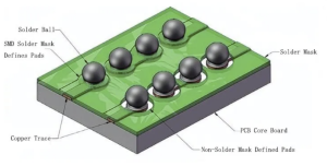
What Are the Key Considerations for Solder Mask Application?
- Screen Printing
Screen printing uses a stencil. The stencil has small holes. Green ink passes through. It covers the board. The process needs accuracy. It uses a squeegee. The squeegee spreads the ink. It moves fast. The ink fills the gaps. This method is quick. Screen printing needs high pressure.
The pressure ensures good coverage. The board is then dried. Operators check for errors. They make sure the ink is even. Each board must look perfect. It protects the board. - Spray Coating
Spray coating uses a machine. The machine sprays green ink. Tiny drops cover the board. It moves fast and even. The pressure is high. This ensures good coverage. The ink sticks well. Operators control the speed. The board is then baked. Baking makes the ink hard.
This process is smooth. Spray coating covers all parts. It needs careful handling. The machine must be clean. No dust should mix. Operators check the board. They look for thin spots. Spray coating is precise. It’s used in PCB fab. - Adhesion
Adhesion is important. The solder mask must stick. Clean the board first. Dirt and oil affect adhesion. Use chemicals to clean. This makes the surface ready. Apply the mask next. It sticks better now. Check the board for bubbles. Bubbles weaken adhesion. Press the mask down.
This removes air. Bake the board to finish. Heat makes the mask stick. Good adhesion protects the board. Operators check the bond. They make sure it’s strong. This ensures quality. - Coverage
Coverage is critical. The solder mask must be covered well. Apply the mask evenly. Use the right amount. No gaps should show. The board needs full coverage. It protects from short circuits. Inspect the mask after application. Look for thin areas. Fix any spots missed. Operators use special tools.
They ensure even layers. The mask must cover all traces. Good coverage means safety. It’s part of quality control. Coverage helps in PCB fab. This step is vital for China PCB manufacturing. - UV Curing
UV curing uses light. The board goes under a UV lamp. The light is strong. It hardens the solder mask. This process is fast. The mask dries quickly. UV curing needs precise timing.
Too long weakens the mask. Operators set the timer. The board must be clean. Dust affects curing. This step ensures durability. The mask becomes tough. It sticks well. UV curing is reliable. It’s used in PCB fab. The board is then ready. UV curing makes the mask last.
How to Select the Best Surface Finishing Techniques?
- HASL
HASL stands for Hot Air Solder Leveling. It uses molten solder. The board dips into the solder. Hot air blows off the extra. The process ensures even coating. It needs a precise temperature. Operators check for a smooth finish. HASL provides good solderability. The thickness is consistent.
This method is common. Boards are protected from oxidation. It’s reliable and effective. HASL is used in many PCBs. They handle various components. It’s important for connections. The board stays durable. Quality control checks are frequent. HASL helps make strong PCBs. - ENIG
ENIG stands for Electroless Nickel Immersion Gold. It uses two layers. The first is nickel. The second is gold. The process starts with cleaning. The board dips in a nickel solution. Then it dips into gold. Nickel provides strength. Gold prevents oxidation. This method is precise.
It needs careful control. The layers are thin. It’s used for fine-pitch components. The board gets a flat surface. This process ensures reliability. Operators check for defects. ENIG is common in high-tech PCBs. It improves durability. This method is trusted. Quality is always checked. - OSP stands for Organic Solderability Preservative. It uses a thin organic layer. The board is cleaned first. Then it dips into the OSP solution. The layer bonds to copper. It needs precise control. OSP protects from oxidation. It’s used for short-term protection.
The layer is very thin. Operators check for coverage. OSP is eco-friendly. It’s used in many PCBs. This method is low-cost. The process must be clean. OSP helps in reliable connections. It’s essential for good soldering. - Immersion Tin
Immersion Tin coats the board with tin. The process starts with cleaning. The board dips in tin solution. Tin bonds to copper. The layer is thin and even. It’s important for fine-pitch components. Operators control time and temperature.
They ensure quality coating. Immersion Tin is eco-friendly. It’s used in many PCBs. The process needs careful handling. Tin protects from oxidation. Quality checks are frequent. The board must be smooth. Immersion Tin helps make strong connections. - Immersion Silver
Immersion Silver adds a silver layer. The board is cleaned first. It dips in silver solution. Silver bonds to copper. The layer is thin and smooth. It’s important for high-frequency signals. Operators control the process. They check for even coating.
Immersion Silver is eco-friendly. It’s used in many PCBs. This method prevents oxidation. Silver is very conductive. Quality checks are essential. The board must be clean. Immersion Silver ensures reliable connections. It’s vital in advanced PCBs.
Conclusion
You learned about the PCB Fab process. Drilling, plating, and finishing steps are key. Using these tips will help make good boards. Always check each step. Master these tips for the best results. Visit LHD-PCB for more. Happy building!
0