4 Advanced Routing Techniques for Multilayer PCB
Home » 4 Advanced Routing Techniques for Multilayer PCB
RECENT POSTS
Share:
- December 9, 2024
Table of Contents
Advanced Routing Techniques for Multilayer PCB
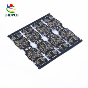
In the ever-evolving world of electronics, Printed Circuit Boards (PCBs) play a critical role in connecting and managing complex electrical components. As technology advances and functionalities become more intricate, the demand for high-performance PCBs increases. This is where the multilayer PCB enters as a sophisticated solution offering exceptional capabilities for demanding applications.

Advantage of Multilayer PCB
Unlike traditional single-layer or double-layer PCBs, multilayer PCB boasts a structure with multiple conductive layers stacked and interconnected through vias. This increased layer count allows for significant benefits:

- Higher Component Density: More layers translate to more space for routing signals and placing components, enabling compact and efficient PCB designs.
- Enhanced Performance: The shorter signal paths within multilayer PCBs minimize signal loss and improve overall circuit performance.
- Reduced Crosstalk: Strategic layer arrangements and routing techniques can significantly reduce crosstalk, a phenomenon where electrical signals from one trace interfere with another.
However, maximizing the advantages of multilayer PCBs hinges on effective routing techniques. Here’s a closer look at some advanced strategies employed by PCB design professionals:
1. Impedance Control: Impedance refers to the opposition a circuit presents to alternating current (AC) signals. Maintaining consistent impedance throughout a signal path is crucial for signal integrity and avoiding reflections or distortions. In multilayer PCBs, designers leverage various techniques to achieve controlled impedance, such as:
- Trace Width and Spacing Adjustments: Adjusting the width and spacing of signal traces directly affects their impedance. By carefully calculating and implementing these adjustments, designers can ensure optimal signal transmission.
- Dielectric Layer Thickness Control: The thickness and material properties of the dielectric layers separating conductive layers also influence impedance. Selecting appropriate materials and carefully managing layer thicknesses is essential for impedance control.
2. High-Speed Design Techniques: As data transmission speeds increase, multilayer PCBs require specialized design considerations for high-frequency signals. Some common techniques include:
- Differential Pair Routing: When dealing with high-speed differential signals, routing these signals in tightly coupled pairs helps cancel out common-mode noise and maintain signal integrity.
- Coplanar Waveguides: These specialized routing structures provide a controlled environment for high-frequency signals, minimizing losses and ensuring reliable data transmission.
3. Advanced Via Management: Via are tiny holes connecting different conductive layers within a multilayer PCB. Their placement and configuration significantly impact signal integrity. Here’s how advanced via management techniques come into play:
- Via Minimization: While via are essential for interlayer connections, excessive via can introduce parasitic capacitance and inductance, degrading signal performance. Designers strive to minimize the number of via while maintaining full functionality.
- Via Stacking: The strategic placement of via in different layers can help mitigate crosstalk and signal integrity issues. Techniques like via staggering and controlled via placement play a crucial role in achieving optimal performance.
4. Design Automation Tools: The intricate nature of multilayer PCB routing often necessitates the use of advanced design automation tools. These software programs offer features like:
- Automated Routing: Specialized algorithms can suggest optimal routing paths based on the designer’s defined rules and constraints.
- Impedance Calculation and Simulation: Design tools can analyze the impedance characteristics of different routing scenarios, allowing designers to optimize for consistent impedance.
- 3D Visualization: Visualization tools help designers visualize the complete layout of the multilayer PCB, ensuring proper clearance between components and routing paths.
Effective routing techniques are the cornerstone of maximizing the potential of multilayer PCBs. By employing these advanced strategies, designers can optimize signal paths, minimize crosstalk, and ensure exceptional performance for even the most demanding applications.
0


